Why in the f#%k would you make an 8-bit breadboard computer?
Part of who I am as a person is my curosity and urge to figure out how complex systems work. In the modern software realm, it’s common practice to abstract everything possible away from programmers. The common explaination for this is that programmers don’t necessarily need to be bogged down with all of these details. To be clear, I don’t think that you have to necessarily learn about hardware as a programmer; however, I do think that learning about it can provide different ways of thinking about how to write code.
It seems like at one point in time, it was almost necessary to understand these things in order to even be a programmer; however, as hardware speed increased there was a decrease with the concern of how hardware works among the majority of programmers. Making it almost kind of a lost art for the majority of programmers.
This project was my commitment to continous learning, self-improvement, and the dedication to myself to always remain curious.
The Journey to Complete
A few years ago, I stumbled upon Ben Eaters youtube channel that contained a bunch of amazing videos. One of the series that Ben produced was an 8-bit breadboard computer series, which at the time I have no idea what that even meant. I watched a few of the videos and felt a bit intimidated, so instead of picking up any of the kits and starting the project I figured I’d try to learn a bit more about general computer architecture. Holy s%!t, talk about being thrown in to the deep end of the pool filled with sharks and carrying a baby.
I didn’t even really know where to start, so I just began searching the internet. Luckily, at the time I was messing around with some Raspberry Pi’s for home automation stuff and came across a pretty amazing book Learning Computer Architecture with Raspberry Pi. If you have no prior computer architecture experience, I can’t recommend this book enough. Pick up a copy, read it, re-read it, and read it again. It helped me build the confidence that I needed in order to pick up the 8-bit breadboard computer kit and build it.
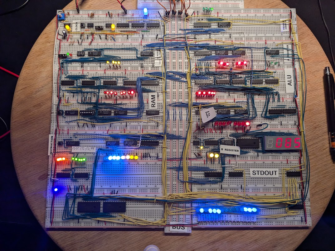
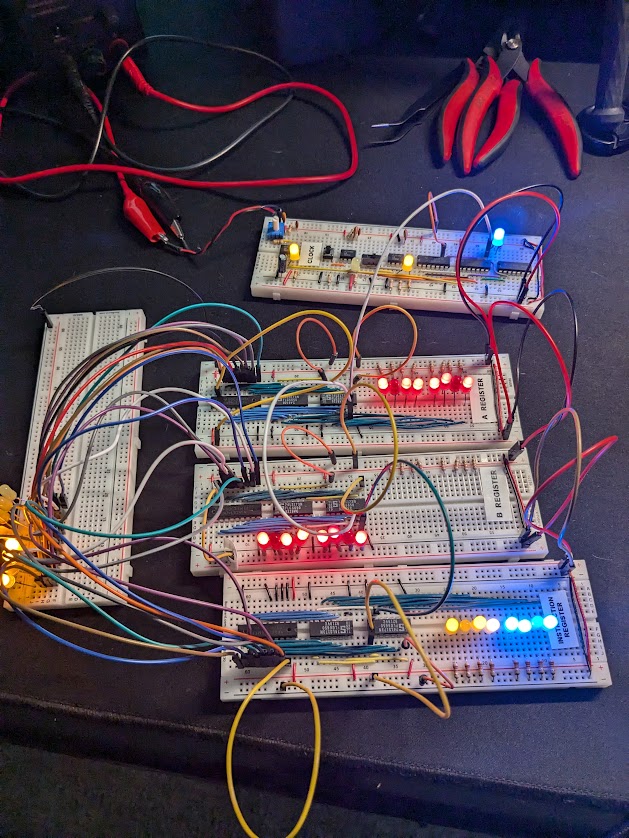
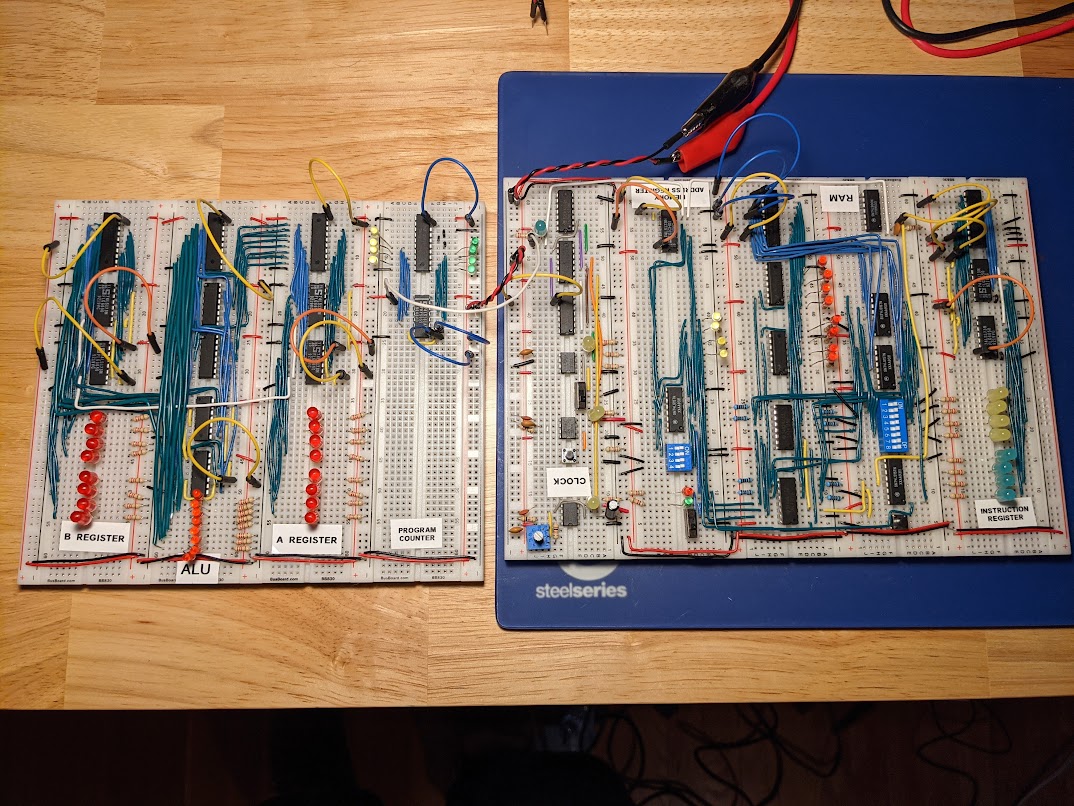
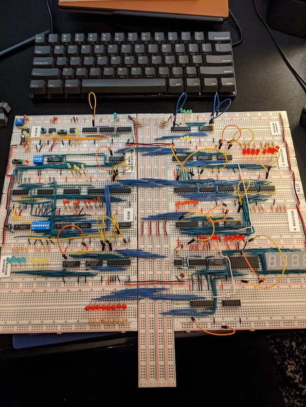
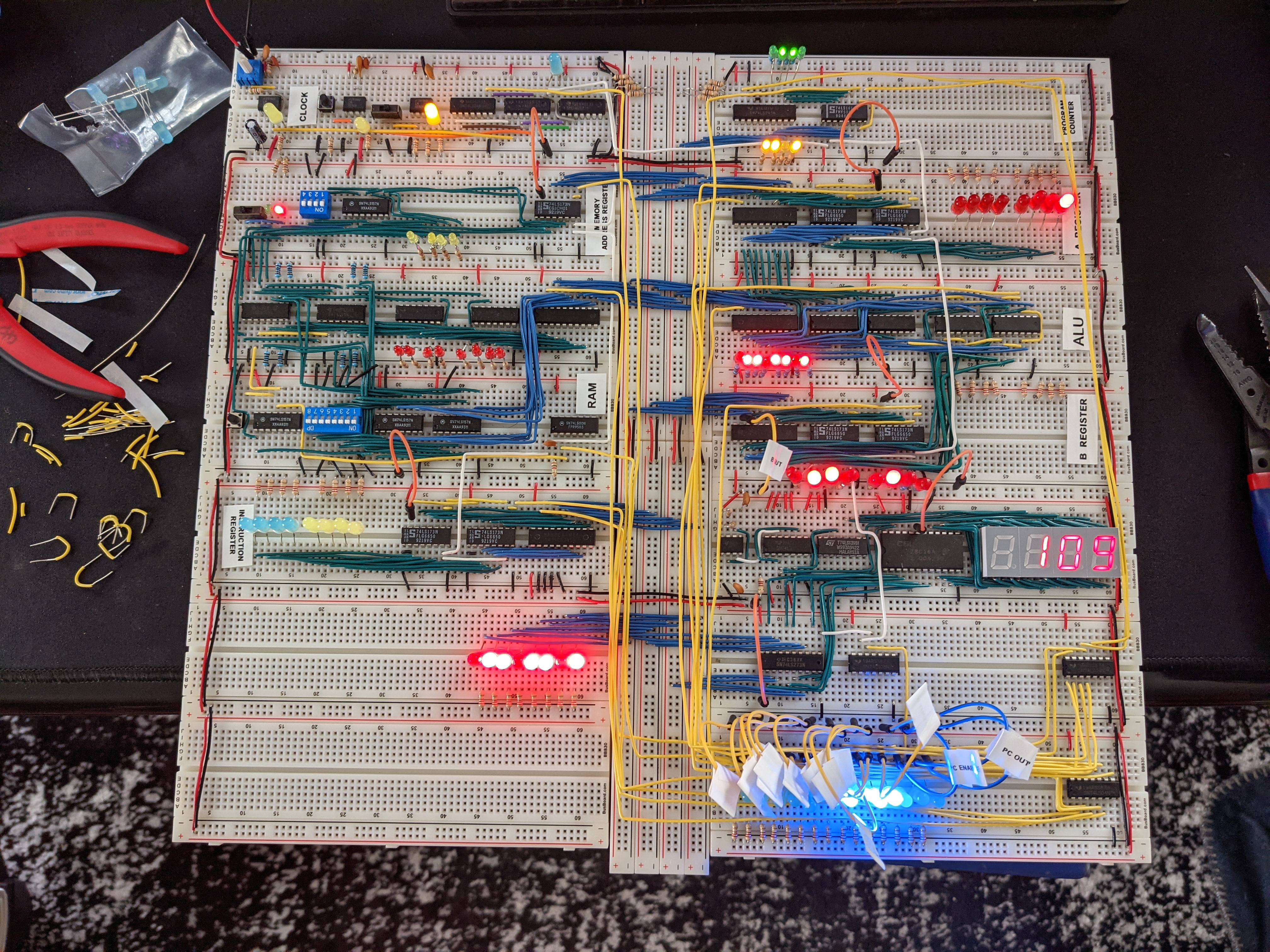
Fast forward a few years later around November 2020, I decided that I was going to purchse the 8-bit breadboard computer kit as a birthday present to myself. The kit came with three modules, the Clock Module, Register and ALU Module, The Ram and Program Counter Module, and the Output and Control Logic Module. I didn’t have a few other things that Ben had, so needless to say I picked up more than what was necessary just to be able to have it on hand. I was excited about starting the project and expanding my knowledge on computer architecture.
I took my time with each module watching the tutorial videos that Ben created, watching videos on basic electricity concepts like the differences between voltage, current, amperage, and wattage, learning how to use a multimeter, learning how to use an oscilloscope, learning different basic logic gates, learning about latches and flip-flops, learning how to read schmatics, and a lot more. The breadth of knowledge that I accquired during my initial attempt at building the 8-bit breadboard computer was amazing.
Something that was stated in that last sentence is really important, I said “… during my initial attempt …”. Life happens, and we all know it. I started the project in late 2020 and got to the third module in early 2021, but my personal life was a wreck. I had to put a lot of my hobbies and learning on pause in order to fix things in my daily life. So, here I am, it’s August 2024 and I’ve finally completed the project. I ended up picking it back up in July of 2024 with the goal of putting in as many hours required of freetime to complete the project. I actually took apart all of the modules that I previously built in order to rebuild the entire kit to make sure that everything that I previously learned still stuck around in some neurons in my brain.
It took me a long time from start to finish, but I got it done using a lot of willpower and dedication. There were a lot of instances where I had to debug hardware issues due to bad wires, bad chips, or countless other things. There were times when I was working on the project, that I legitimately just thought I probably should just stop and give up to work on something software related instead; however, I wanted to see it through to the end as a commitment to myself and the journey.
If there is anything to take away from this portion of the article, besides the fact that I might have been driven to the brink of insanity, is that it is imporant to see projects through to the end whatever the end may mean to you. Getting far enough in a project to where you can call it completed or done, feels rewarding and fulfilling. Also, putting something down for the time being doesn’t have to always mean that you are never going to pick it back up to finish it.
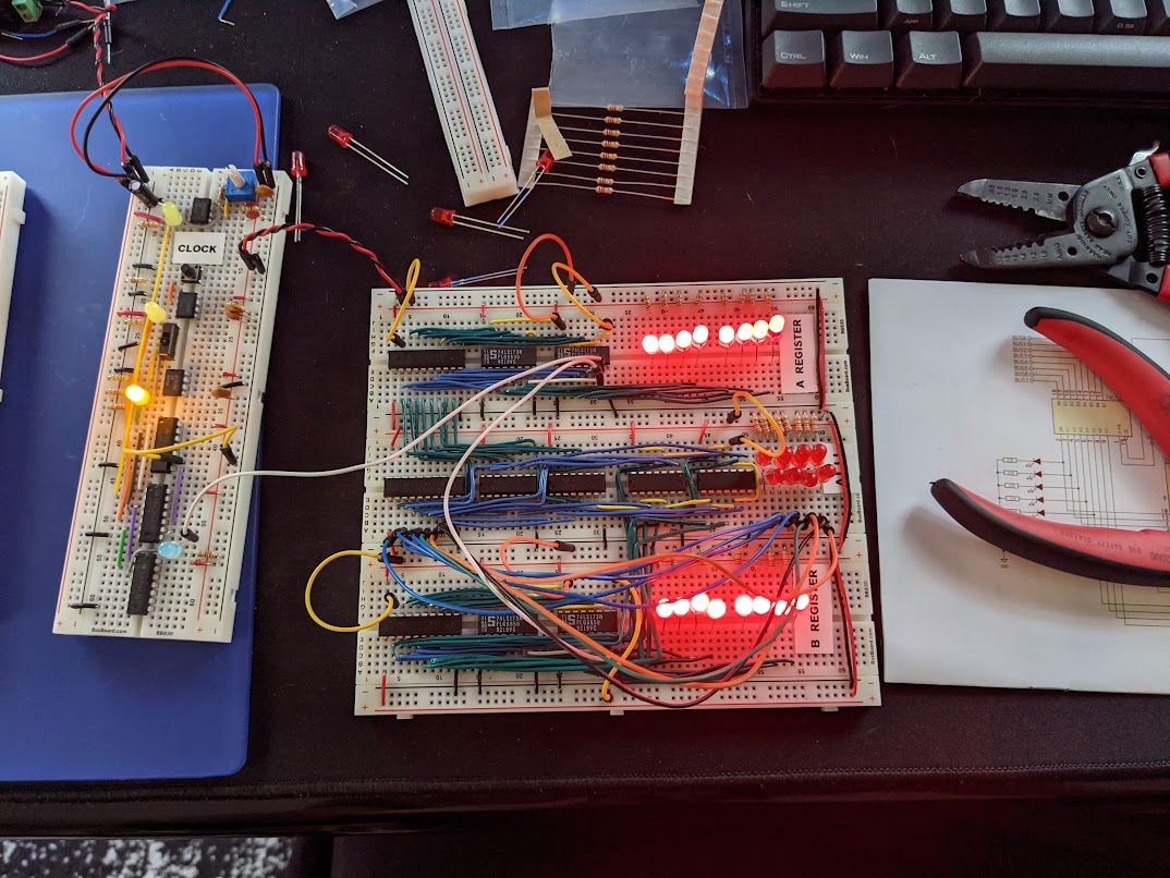
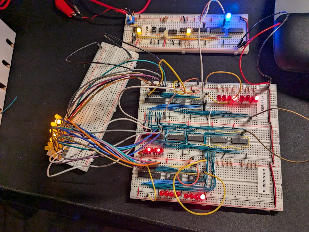
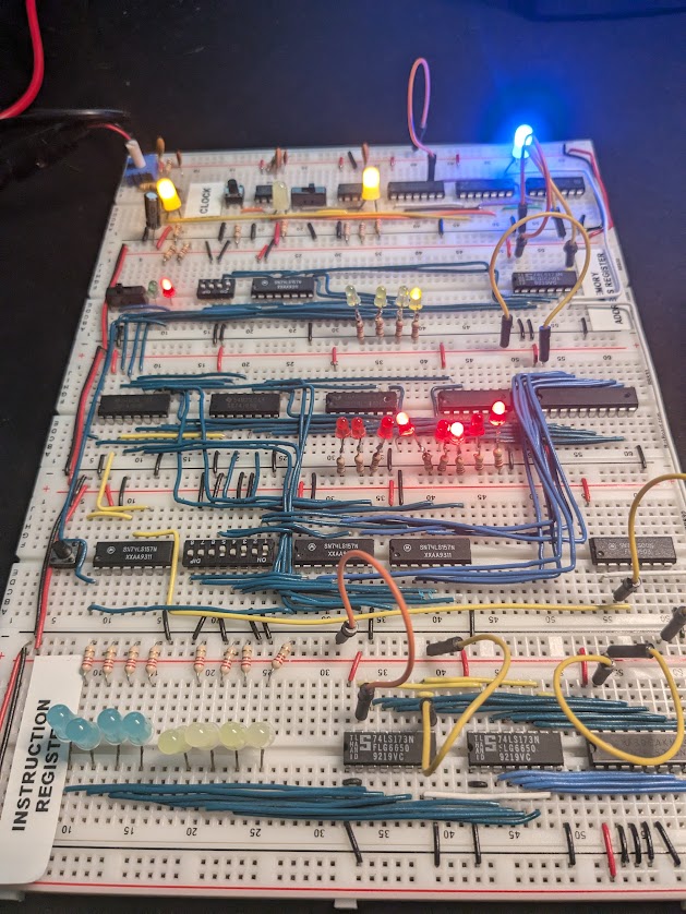
Clock Module
A computer’s main clock is what’s used to synchronize most of the operations in a computer. This computer’s clock
utilizies the 555 timer integrated circuit, and it contains two clocks circuits. An a-stable circuit that continously
plusing with an adjustable speed and a mono-stable circuit that is hooked up to a button that is debounced in order to
help with debugging that can created manual clock pluses with a button push. In order to be able to toggle between the
two, additional components were added with a throw switch to be able to toggle between the two.
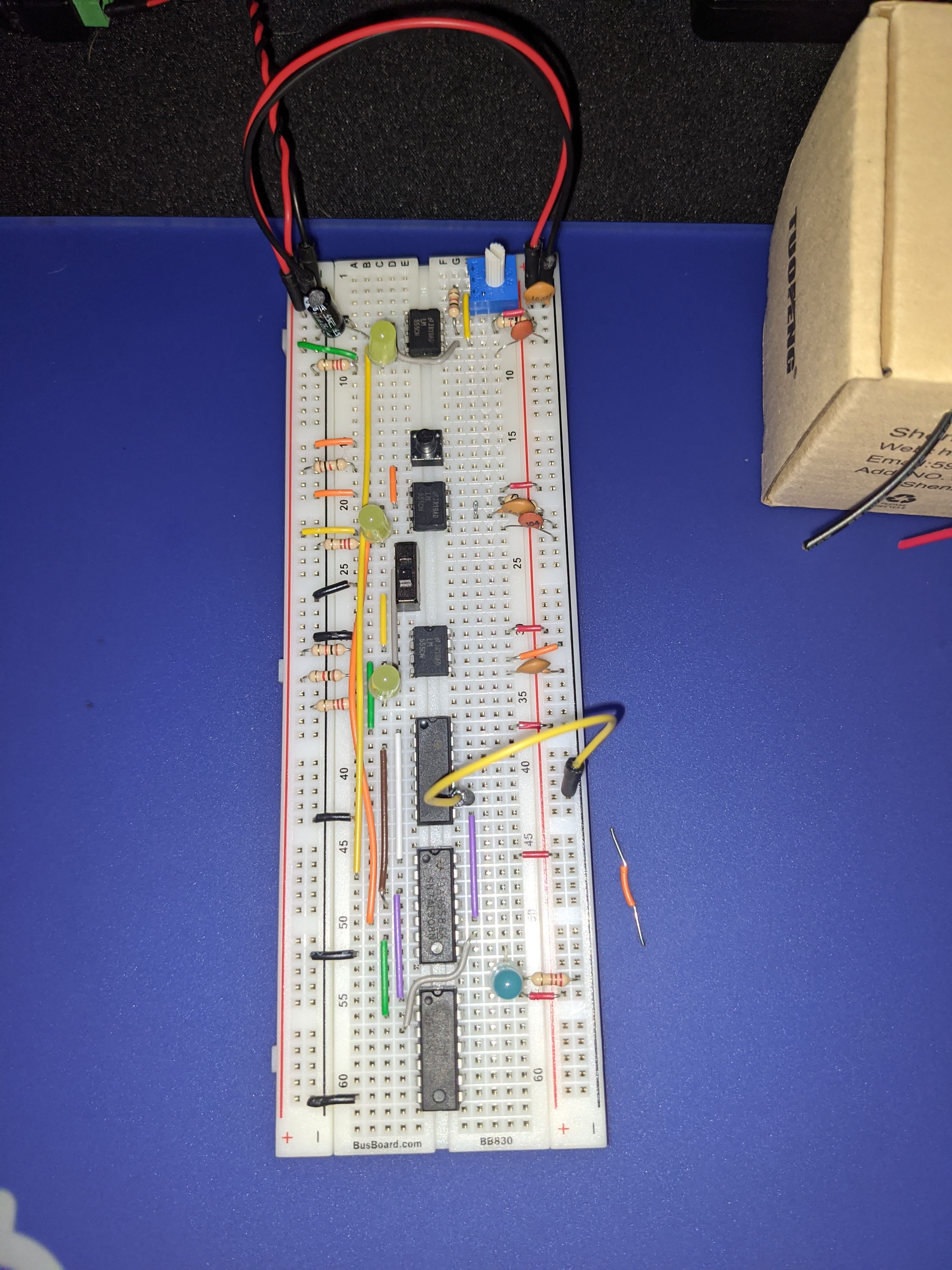
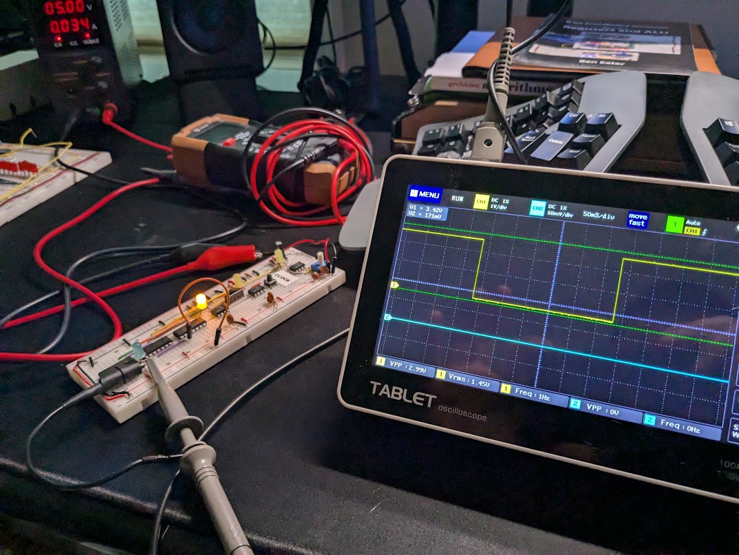
For fun, just like in Ben’s videos, I hook up the clock to an oscilloscope to see what the a-stable clocks output was
after it was hooked up to a capacitor and a few resistors.
We’ll see in later portions that other components might require their own clock to run independently of the main computer’s clock.
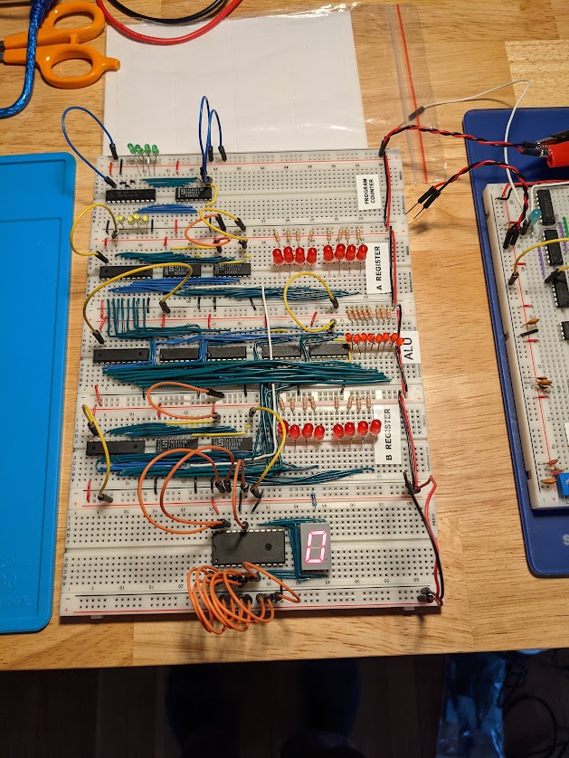
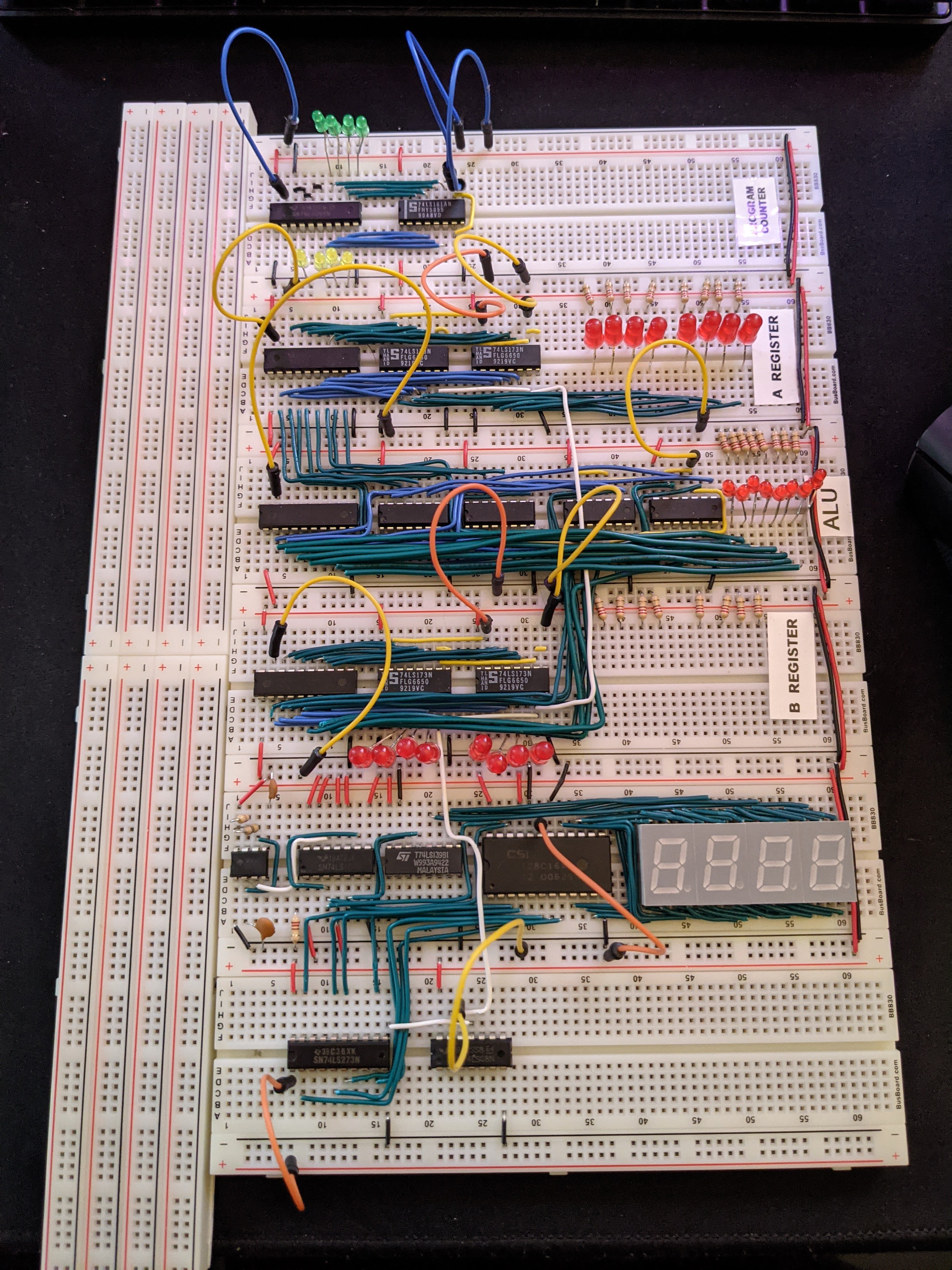
Registers and ALU
This computer contains a few different 8-bit registers, for this particular module the A Register, B Register,
and Instruction Register. The A and B registers will be used for storing data and wired up to the Arithmetic
Logic Unit. Each 8-bit register is comprised of two 4-bit registers that are connected to a a octal bus transceiver,
which we’ll be using a bunch in this project in order to place or read signals on and off the bus.
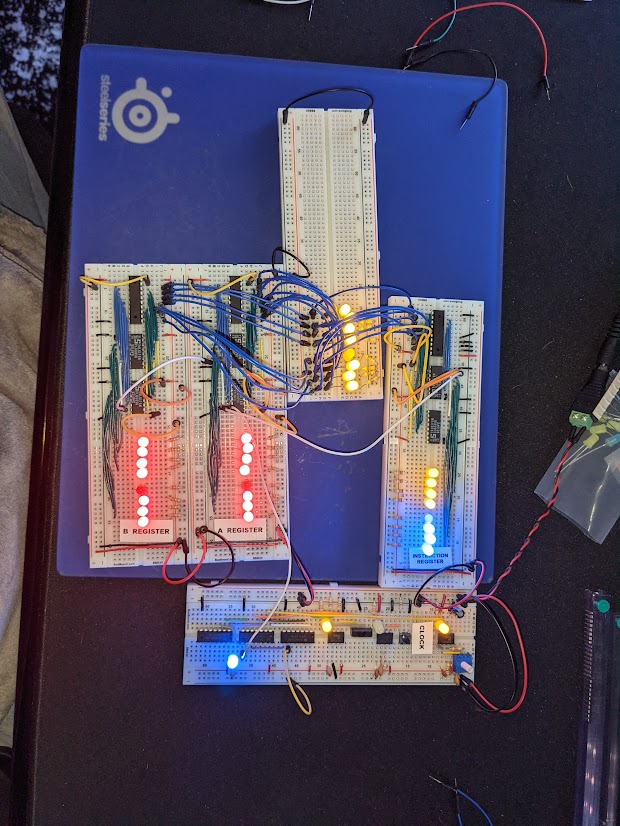
Building out all of these components required a lot of manual testing and a mess of jumper wires. I’d often set up
a test breadboard with jumper wires that connected to multiple components to a bus to move data between the components
or as a way to just test particular signals or pieces.
After hooking up and testing out each of the registers, the ALU was next on the list of components to build. Instead
of manually building out an adder, the kit just utilizied another 4-bit binary adder integrated circuit. All that was
needed to be done was wiring up the carry pin of the first 4-bit adder to the input of the second 4-bit adder, then
wiring up all of the inputs to the adders to the A and B registers. In order to also allow subtraction, XOR gates
were wired up to do two-complement addition and subtraction. In order to place values on the bus another octal bus
transceiver was hooked up to the ALU.
For these components, a common test that I preformed was hooking up the both registers to a temporary bus breadboard,
setting one register to the binary value of b00000001, setting the other register transceiver to read off the bus, and
setting the ALU register to output to the bus. This would continously add the value b00000001 a single register
consequently causing the ALU to update with a new value.
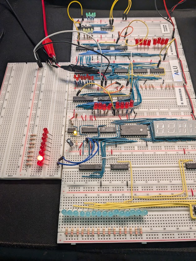
RAM and Address Register
Every computer needs some form of memory or temporary storage, and mechanism to figure out which memory address the
computer needs to fetch data from. The basic build for this component was using a two 64-bit RAM integrated circuit
inverts to invert the output the RAM chips, and octal bus transceiver.
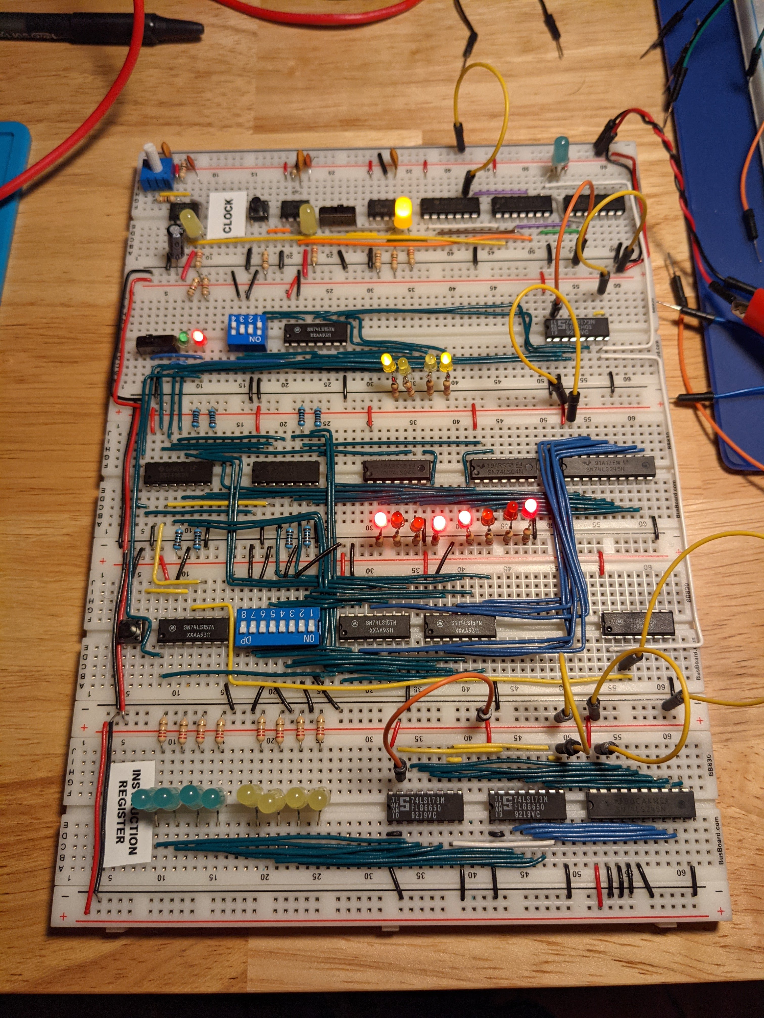
Once the RAM module was built out, another register was needed in order to be able to address our RAM. So another
4-bit register was added with some additional chips and switches to allow for automatic or manually addressing. This
module was then connected to the RAM module.
Another useful piece that was assembled using dip switches and multiplexer was a module below the RAM module that was
connected to the ram. This piece allowed for direct memory writes with the setting of dip switches and the push of a
button when the manual memory address register mode was set to enabled.
Program Counter
A program counter is another important piece of a computer, it will keep track of where we are supposed to be in our
programs that we’ll be manually writing to memory later. For this piece, a basic 4-bit counter chip was used as well
as another transceiver. To test out the counter, I wired up to the main computer clock to ensure that it was working as
expected.
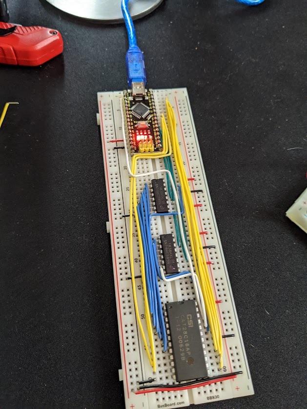
EEPROM Programmer
In this project, EEPROMs (electronical erasable programmable read-only memory) are used for a few different pieces.
They are used as a replacement for combinational logics or basically a decoder. Using an adruino nano with some 8-bit
shift registers in order to expand the amount of data that we can write to the EEPROM due to the limited amount of pins
on the arduino nano.
Below is a test program that was used to ensure that the data was being shifted properly, each of the shift register were hooked up to a test bus with LEDs.
#define SHIFT_DATA 2
#define SHIFT_CLK 3
#define SHIFT_LATCH 4

void setup() {
  pinMode(SHIFT_DATA, OUTPUT);
  pinMode(SHIFT_CLK, OUTPUT);
  pinMode(SHIFT_LATCH, OUTPUT);

  shiftOut(SHIFT_DATA, SHIFT_CLK, MSBFIRST, 0x55); // 0x55 -> 01010101
  shiftOut(SHIFT_DATA, SHIFT_CLK, MSBFIRST, 0x55);

  digitalWrite(SHIFT_LATCH, LOW);
  digitalWrite(SHIFT_LATCH, HIGH);
  digitalWrite(SHIFT_LATCH, LOW);
}

void loop() {}
Once the programmer was assembled, an EEPROM is popped in and and wired up with the appropriate lines for addressing, IO, output enable, and write enable. This programmer just allows use to address memory on the EEPROM and write to it programmatically by updating the microcontroller code to be able to address and write data to the EEPROM.
#define SHIFT_DATA 2
#define SHIFT_CLK 3
#define SHIFT_LATCH 4
#define EEPROM_D0 5
#define EEPROM_D7 12
#define WRITE_EN 13

void setAddress(int address, bool outputEnabled) {
  shiftOut(SHIFT_DATA, SHIFT_CLK, MSBFIRST,
  (address >> 8) | (outputEnabled ? 0x00 : 0x80));
  shiftOut(SHIFT_DATA, SHIFT_CLK, MSBFIRST, address);
  digitalWrite(SHIFT_LATCH, LOW);
  digitalWrite(SHIFT_LATCH, HIGH);
  digitalWrite(SHIFT_LATCH, LOW);
}

byte readEEPROM(int address) {
  for (int pin = EEPROM_D0; pin <= EEPROM_D7; pin += 1) {
    pinMode(pin, INPUT);
  }
  setAddress(address, true);
  byte data = 0;
  for (int pin = EEPROM_D7; pin >= EEPROM_D0; pin -= 1) {
    data = (data << 1) + digitalRead(pin);
  }
  return data;
}

void writeEEPROM(int address, byte data) {
  for (int pin = EEPROM_D0; pin <= EEPROM_D7; pin += 1) {
    pinMode(pin, OUTPUT);
  }
  setAddress(address, false);
  for (int pin = EEPROM_D0; pin <= EEPROM_D7; pin += 1) {
    digitialWrite(pin, data & 1);
    data = data >> 1;
  }
  digitalWrite(WRITE_EN, LOW);
  delayMicroseconds(1);
  digitalWrite(WRITE_EN, HIGH);
  delay(10);
}

void printContents() {
  for (int base = 0; base <= 255; base += 16) {
    byte data[16];
    for (int offset = 0; offset <= 15; offset += 1) {
      data[offset] = readEEPROM(base + offset);
    }
    char buf[80];
    sprintf(buf,
        "%03x:  "
        "%02x %02x %02x %02x %02x %02x %02x %02x"
        "%02x %02x %02x %02x %02x %02x %02x %02x",
        base, data[0], data[1], data[2],
        data[3], data[4], data[5], data[6],
        data[7], data[8], data[9], data[10],
        data[11], data[12], data[13], data[14], data[15]);
    Serial.println(buf);
  }
}

void setup() {
  pinMode(SHIFT_DATA, OUTPUT);
  pinMode(SHIFT_CLK, OUTPUT);
  pinMode(SHIFT_LATCH, OUTPUT);
  digitalWrite(WRITE_EN, HIGH);
  pinMode(WRITE_EN, OUTPUT);
  Serial.begin(57600);
  for (int address = 0; address <= 255; address += 1) {
    writeEEPROM(address, 0x00);
  }
  printContents();
}

void loop() {}
Hex Display
To avoid going insane from reading random LEDs on the board and translating them to their binary value to decimal value. Seven segment hex displays were added to the computer to be able to get some form of different visual feedback. Cleverly, EEPROMs were used as a decoder to be able to take in an address and output the appropriate binary value to light up the hex displays. The decoder tables looked like the following:
| Hex | Binary | A B C D E F G |
|---|---|---|
| 0 | 0000 | 0 0 0 0 0 0 1 |
| 1 | 0001 | 1 0 0 1 1 1 1 |
| 2 | 0010 | 0 0 1 0 0 1 0 |
| 3 | 0011 | 0 0 0 0 1 1 0 |
| 4 | 0100 | 1 0 0 1 1 0 0 |
| 5 | 0101 | 0 1 0 0 1 0 0 |
| 6 | 0110 | 0 1 0 0 0 0 0 |
| 7 | 0111 | 0 0 0 1 1 1 1 |
| 8 | 1000 | 0 0 0 0 0 0 0 |
| 9 | 1001 | 0 0 0 0 1 0 0 |
| A | 1010 | 0 0 0 1 0 0 0 |
| B | 1011 | 1 1 0 0 0 0 0 |
| C | 1100 | 0 1 1 0 0 0 0 |
| D | 1101 | 1 0 0 0 0 1 0 |
| E | 1110 | 0 1 1 0 0 0 0 |
| F | 1111 | 0 1 1 1 0 0 0 |
Using the EEPROM programmer that was previously build, the truth table can be written to an EEPROM that is than hooked up to several four segment hex displays.
#define SHIFT_DATA 2
#define SHIFT_CLK 3
#define SHIFT_LATCH 4
#define EEPROM_D0 5
#define EEPROM_D7 12
#define WRITE_EN 13

void setAddress(int address, bool outputEnable) {
  shiftOut(SHIFT_DATA, SHIFT_CLK, MSBFIRST,
    (address >> 8) | (outputEnable ? 0x00 : 0x80));
  shiftOut(SHIFT_DATA, SHIFT_CLK, MSBFIRST, address);
  digitalWrite(SHIFT_LATCH, LOW);
  digitalWrite(SHIFT_LATCH, HIGH);
  digitalWrite(SHIFT_LATCH, LOW);
}

byte readEEPROM(int address) {
  for (int pin = EEPROM_D0; pin <= EEPROM_D7; pin += 1) {
    pinMode(pin, INPUT);
  }
  setAddress(address, true);
  byte data = 0;
  for (int pin = EEPROM_D7; pin >= EEPROM_D0; pin -= 1) {
    data = (data << 1) + digitalRead(pin);
  }
  return data;
}

void writeEEPROM(int address, byte data) {
  setAddress(address, /*outputEnable*/ false);
  for (int pin = EEPROM_D0; pin <= EEPROM_D7; pin += 1) {
    pinMode(pin, OUTPUT);
  }
  for (int pin = EEPROM_D0; pin <= EEPROM_D7; pin += 1) {
    digitalWrite(pin, data & 1);
    data = data >> 1;
  }
  digitalWrite(WRITE_EN, LOW);
  delayMicroseconds(1);
  digitalWrite(WRITE_EN, HIGH);
  delay(10);
}

void printContents() {
  for (int base = 0; base <= 255; base += 16) {
    byte data[16];
    for (int offset = 0; offset <= 15; offset += 1) {
      data[offset] = readEEPROM(base + offset);
    }
    char buf[80];
    sprintf(buf,
        "%03x:  "
        "%02x %02x %02x %02x %02x %02x %02x %02x"
        "%02x %02x %02x %02x %02x %02x %02x %02x",
        base, data[0], data[1], data[2],
        data[3], data[4], data[5], data[6],
        data[7], data[8], data[9], data[10],
        data[11], data[12], data[13], data[14], data[15]);
    Serial.println(buf);
  }
}

void setup() {
  pinMode(SHIFT_DATA, OUTPUT);
  pinMode(SHIFT_CLK, OUTPUT);
  pinMode(SHIFT_LATCH, OUTPUT);
  digitalWrite(WRITE_EN, HIGH);
  pinMode(WRITE_EN, OUTPUT);
  Serial.begin(57600);
  byte digits[] = {
      0x7e, 0x30, 0x6d, 0x79,
      0x33, 0x5b, 0x5f, 0x70,
      0x7f, 0x7b
  };
  Serial.println("Programming ones place");
  for (int value = 0; value <= 255; value += 1) {
    writeEEPROM(value, digits[value % 10]);
  }
  Serial.println("Programming tens place");
  for (int value = 0; value <= 255; value += 1) {
    writeEEPROM(value + 256, digits[(value / 10) % 10]);
  }
  Serial.println("Programming hundreds place");
  for (int value = 0; value <= 255; value += 1) {
    writeEEPROM(value + 512, digits[(value / 100) % 10]);
  }
  Serial.println("Programming sign");
  for (int value = 0; value <= 255; value += 1) {
    writeEEPROM(value + 768, 0);
  }
  Serial.println("Programming ones place (twos complement)");
  for (int value = -128; value <= 127; value += 1) {
    writeEEPROM((byte)value + 1024, digits[abs(value) % 10]);
  }
  Serial.println("Programming tens place (twos complement)");
  for (int value = -128; value <= 127; value += 1) {
    writeEEPROM((byte)value + 1280, digits[abs(value / 10) % 10]);
  }
  Serial.println("Programming hundreds place (twos complement)");
  for (int value = -128; value <= 127; value += 1) {
    writeEEPROM((byte)value + 1536, digits[abs(value / 100) % 10]);
  }
  Serial.println("Programming sign (twos complement)");
  for (int value = -128; value <= 127; value += 1) {
    if (value < 0) {
      writeEEPROM((byte)value + 1792, 0x01);
    } else {
      writeEEPROM((byte)value + 1792, 0);
    }
  }
  Serial.println("Reading EEPROM");
  printContents();
}

void loop() {}
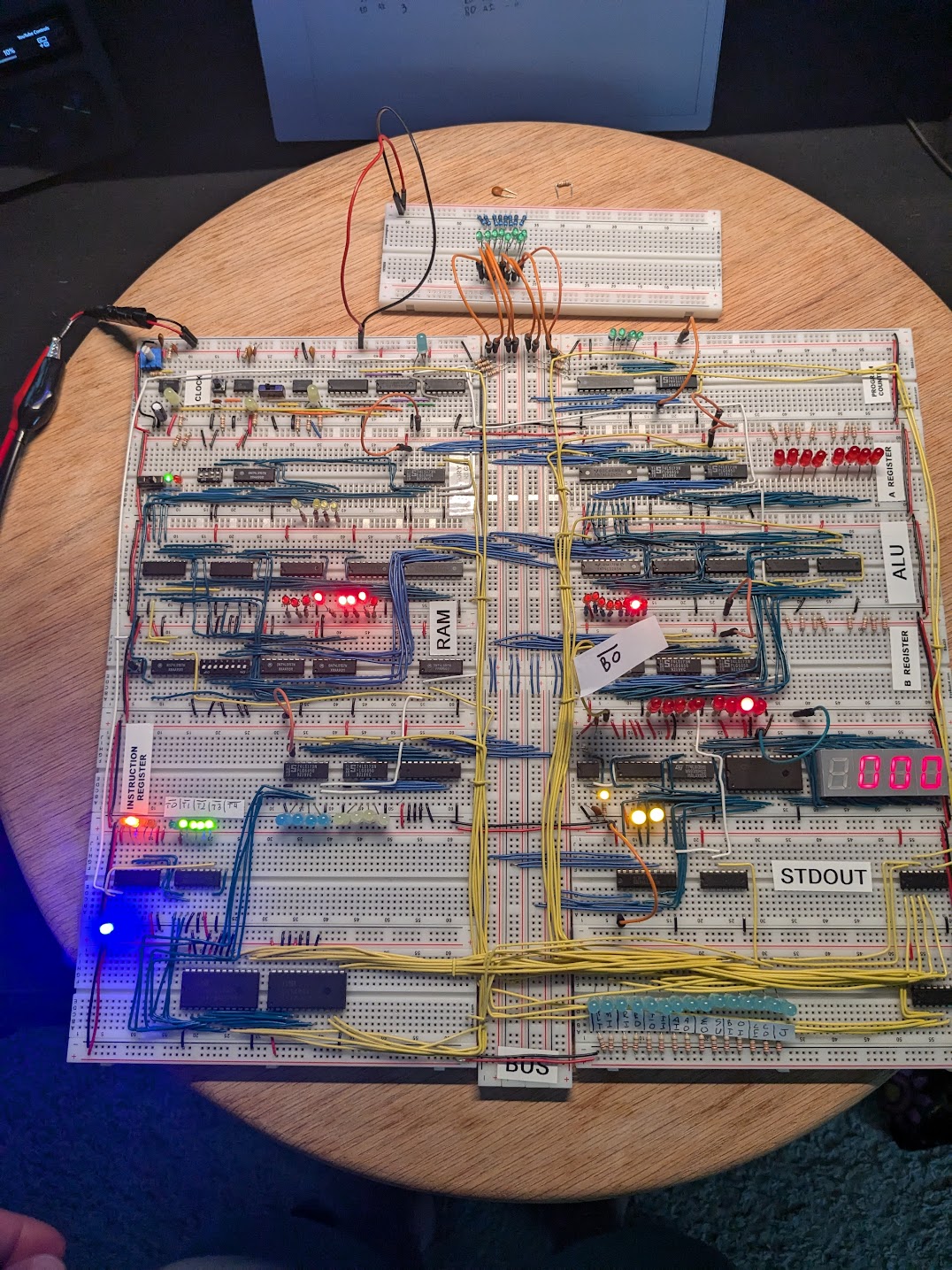
The Bus
In order to have the modules be able to communicate with each other, a bus needs to be created to be able to write to or read from the bus from one component to other. In other words, a pathway was needed in which data can be transfered from one module to another. This would also support control signals that will be our microcode. For this project, what that means in reusing some of the power rails that were removed from breadboards, linking them together, and hooking up the transceivers to the bus as a means to output data or input data from a particular module.
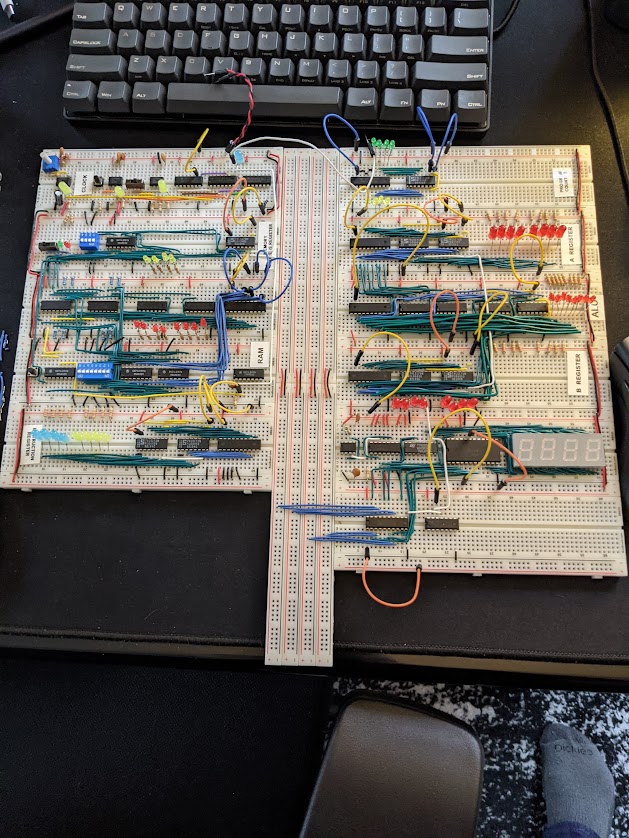
After all of the individual components that had transceivers were hooked up to the bus, relocation of all of the control signals for each of the individual chips where moved to the bottom right of the computer. Since I was still manually testing out the computer, all of the jumps wires were relocated down to the bottom with LEDs to show which signals were enabled. Inverter chips were also used for chips that required an inverted input signal. This helped me with debugging before adding in the control unit.
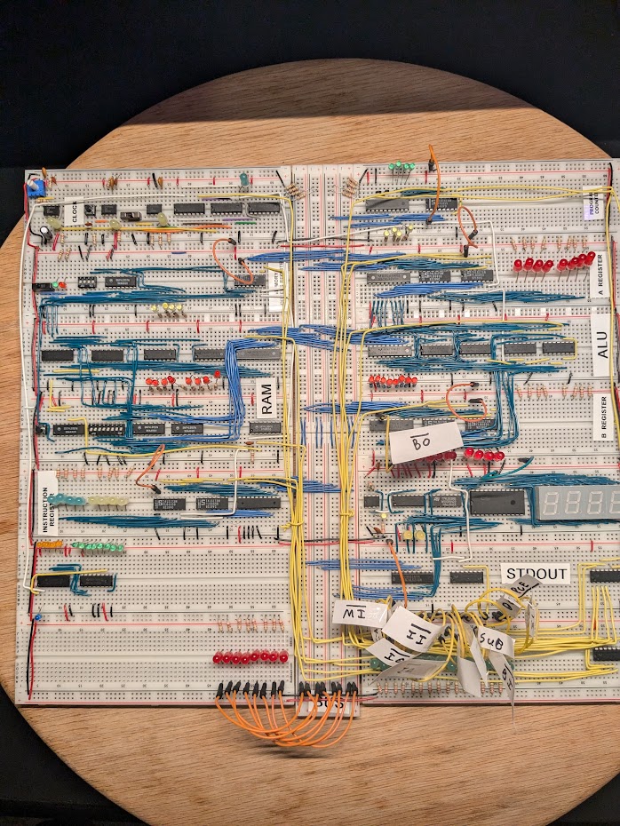
Control Logic
After all of the control signals have been relocated, having a way to control all of these signals through reading a
4-bit instruction from the instruction register, decoding the instruction to a series of control signals, and executing
the series of control signals on a separate counter was the next step towards making the computer programmable.
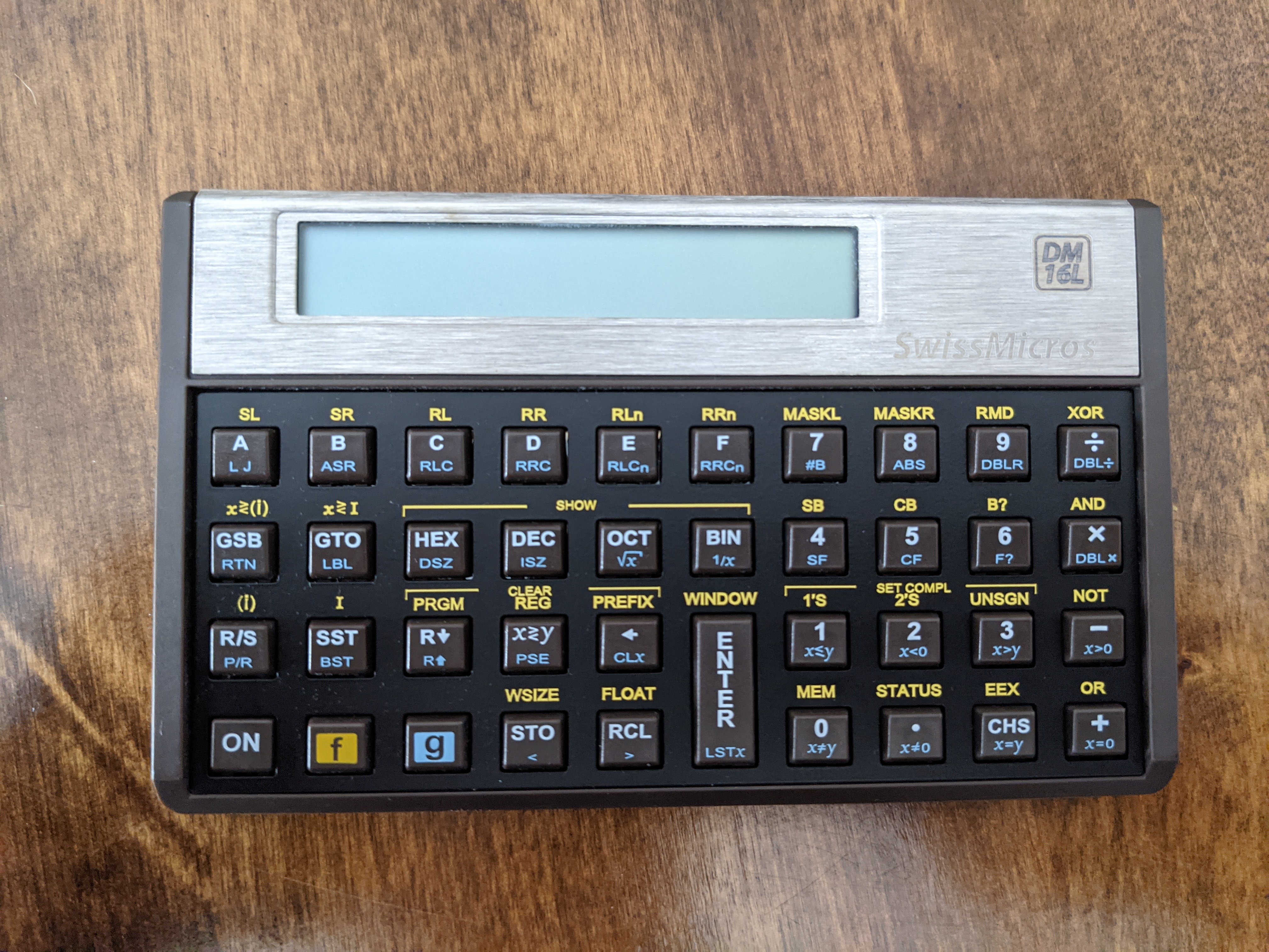
In the series, Ben used an HP16 calculator to assist with doing some binary math. These calculators seem to
have been discontinued for awhile, but I did find a replicate style calculator made by a brand called
SwissMicros. I picked up the DM16L calculator, and I’ve used it a bunch during this portion of
the project.
Microcode and Assembly
Prior to completing this part of the project, I’d had previously read and heard about microcode; however, I had no idea what it actually meant. The amount of clarity that this provided on the topic during this portion of the project was worth all of the struggling and debugging alone. What is microcode? If you take a look at the wiki article on microcode, and you’re like me the explaination of what microcode is on this article was lackluster at best. The way that Ben describe microcode and how it’s related to assembly is one of the best explainations that I’ve ever seen.
Every computer has a particular language that it speaks, in this project we get to basically write the language that
this computer speaks. We’re going to create assembly instructions that map to a series of control logic switches.
The decoding between the assembly instruction and the series of microcode (control logic switches) is another perfect
use case for some EEPROMs. Let’s use simple example of a LDA 14 or LOAD (Memory Address 14) to Register A.
| LDA 14 |
|---|
| Counter-Out, Memory-Address-In |
| RAM-Out, Instruction-Register-In |
| Program-Counter-Enabled |
| Instruction-Register-Out, Memory-Address-In |
| RAM-Out, A-Register-In |
The first three microcode operations are known as a fetch cycle, which job is to fetch the next instruction from the memory address that the program counter current contains. The remaining microcode is the implementation of the assembly instruction.
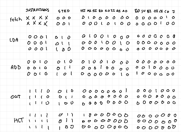
Again, updating the EEPROM microcontroller code to be able to program some EEPROM chips to help with the decoding of instructions to microcode.
#define SHIFT_DATA 2
#define SHIFT_CLK 3
#define SHIFT_LATCH 4
#define EEPROM_D0 5
#define EEPROM_D7 12
#define WRITE_EN 13

#define HLT 0b1000000000000000  // Halt clock
#define MI  0b0100000000000000  // Memory address register in
#define RI  0b0010000000000000  // RAM data in
#define RO  0b0001000000000000  // RAM data out
#define IO  0b0000100000000000  // Instruction register out
#define II  0b0000010000000000  // Instruction register in
#define AI  0b0000001000000000  // A register in
#define AO  0b0000000100000000  // A register out
#define EO  0b0000000010000000  // ALU out
#define SU  0b0000000001000000  // ALU subtract
#define BI  0b0000000000100000  // B register in
#define OI  0b0000000000010000  // Output register in
#define CE  0b0000000000001000  // Program counter enable
#define CO  0b0000000000000100  // Program counter out
#define J   0b0000000000000010  // Jump (program counter in)

uint16_t data[] = {
  MI|CO,  RO|II|CE,  0,      0,      0,         0, 0, 0,   // 0000 - NOP
  MI|CO,  RO|II|CE,  IO|MI,  RO|AI,  0,         0, 0, 0,   // 0001 - LDA
  MI|CO,  RO|II|CE,  IO|MI,  RO|BI,  EO|AI,     0, 0, 0,   // 0010 - ADD
  MI|CO,  RO|II|CE,  IO|MI,  RO|BI,  EO|AI|SU,  0, 0, 0,   // 0011 - SUB
  MI|CO,  RO|II|CE,  IO|MI,  AO|RI,  0,         0, 0, 0,   // 0100 - STA
  MI|CO,  RO|II|CE,  IO|AI,  0,      0,         0, 0, 0,   // 0101 - LDI
  MI|CO,  RO|II|CE,  IO|J,   0,      0,         0, 0, 0,   // 0110 - JMP
  MI|CO,  RO|II|CE,  0,      0,      0,         0, 0, 0,   // 0111
  MI|CO,  RO|II|CE,  0,      0,      0,         0, 0, 0,   // 1000
  MI|CO,  RO|II|CE,  0,      0,      0,         0, 0, 0,   // 1001
  MI|CO,  RO|II|CE,  0,      0,      0,         0, 0, 0,   // 1010
  MI|CO,  RO|II|CE,  0,      0,      0,         0, 0, 0,   // 1011
  MI|CO,  RO|II|CE,  0,      0,      0,         0, 0, 0,   // 1100
  MI|CO,  RO|II|CE,  0,      0,      0,         0, 0, 0,   // 1101
  MI|CO,  RO|II|CE,  AO|OI,  0,      0,         0, 0, 0,   // 1110 - OUT
  MI|CO,  RO|II|CE,  HLT,    0,      0,         0, 0, 0,   // 1111 - HLT
};

void setAddress(int address, bool outputEnable) {
  shiftOut(SHIFT_DATA, SHIFT_CLK, MSBFIRST,
    (address >> 8) | (outputEnable ? 0x00 : 0x80));
  shiftOut(SHIFT_DATA, SHIFT_CLK, MSBFIRST, address);
  digitalWrite(SHIFT_LATCH, LOW);
  digitalWrite(SHIFT_LATCH, HIGH);
  digitalWrite(SHIFT_LATCH, LOW);
}

byte readEEPROM(int address) {
  for (int pin = EEPROM_D0; pin <= EEPROM_D7; pin += 1) {
    pinMode(pin, INPUT);
  }
  setAddress(address, true);
  byte data = 0;
  for (int pin = EEPROM_D7; pin >= EEPROM_D0; pin -= 1) {
    data = (data << 1) + digitalRead(pin);
  }
  return data;
}

void writeEEPROM(int address, byte data) {
  setAddress(address, false);
  for (int pin = EEPROM_D0; pin <= EEPROM_D7; pin += 1) {
    pinMode(pin, OUTPUT);
  }
  for (int pin = EEPROM_D0; pin <= EEPROM_D7; pin += 1) {
    digitalWrite(pin, data & 1);
    data = data >> 1;
  }
  digitalWrite(WRITE_EN, LOW);
  delayMicroseconds(1);
  digitalWrite(WRITE_EN, HIGH);
  delay(10);
}

void printContents() {
  for (int base = 0; base <= 255; base += 16) {
    byte data[16];
    for (int offset = 0; offset <= 15; offset += 1) {
      data[offset] = readEEPROM(base + offset);
    }
    char buf[80];
    sprintf(buf,
        "%03x:  "
        "%02x %02x %02x %02x %02x %02x %02x %02x"
        "%02x %02x %02x %02x %02x %02x %02x %02x",
        base, data[0], data[1], data[2],
        data[3], data[4], data[5], data[6],
        data[7], data[8], data[9], data[10],
        data[11], data[12], data[13], data[14], data[15]);
    Serial.println(buf);
  }
}


void setup() {
  pinMode(SHIFT_DATA, OUTPUT);
  pinMode(SHIFT_CLK, OUTPUT);
  pinMode(SHIFT_LATCH, OUTPUT);
  digitalWrite(WRITE_EN, HIGH);
  pinMode(WRITE_EN, OUTPUT);
  Serial.begin(57600);
  Serial.print("Programming EEPROM");
  for (int address = 0; address < sizeof(data)/sizeof(data[0]); address += 1) {
    writeEEPROM(address, data[address] >> 8);
    if (address % 64 == 0) {
      Serial.print(".");
    }
  }
  for (int address = 0; address < sizeof(data)/sizeof(data[0]); address += 1) {
    writeEEPROM(address + 128, data[address]);
    if (address % 64 == 0) {
      Serial.print(".");
    }
  }
  Serial.println(" done");
  Serial.println("Reading EEPROM");
  printContents();
}

void loop() {}
Turing Complete Computer
Ben also gave a great description of what it means to make a computer Turing complete, or as close as possible to making a computer Turing complete. The famous paper, which states the following:
It is possible to invent a single machine which can be used to compute any computable sequence.
A Turning complete machine reads it’s input from a infinitely long tape that divided in to segments. Each of these segments contains a symbol, a read-head can move back and forth looking at a decode table instructing the machine what to do based on the state it is in. The definition of any computable sequence is a bit vague and Turing admits this in the paper. Ben also shares that this problem was later solved by both Turing and Church in two separate papers.
At this particular moment, the computer that’s being built doesn’t have the ability to do any type of conditional jump. There are instructions for a non-conditional jump that can effectively loop our programs; however, to make this computer more inline with a Turning complete machine a few conditional jump assembly instructions will be needed. This means we’ll need to have some type of state register that can track the state of our machine, this state register is commonly referred to as a flags register.
Flags Register
The computer’s ALU contains a carry bit, this carry bit can be used as a flag and stored in the flags register in order
to implement a jump carry instruction (JC). Using a series of NOR and AND gates to create a zero detecting circuit
from the ALU, which will also be used in the flags register to implement a jump zero instruction (JZ). At this state,
the flags register is still being controlled manually. In order to have our programs automatically set the flag
register, the microcode will be to be updated to set the flag register and contain the new instructions for conditional
jumps.
#define SHIFT_DATA 2
#define SHIFT_CLK 3
#define SHIFT_LATCH 4
#define EEPROM_D0 5
#define EEPROM_D7 12
#define WRITE_EN 13

#define HLT 0b1000000000000000  // Halt clock
#define MI  0b0100000000000000  // Memory address register in
#define RI  0b0010000000000000  // RAM data in
#define RO  0b0001000000000000  // RAM data out
#define IO  0b0000100000000000  // Instruction register out
#define II  0b0000010000000000  // Instruction register in
#define AI  0b0000001000000000  // A register in
#define AO  0b0000000100000000  // A register out
#define EO  0b0000000010000000  // ALU out
#define SU  0b0000000001000000  // ALU subtract
#define BI  0b0000000000100000  // B register in
#define OI  0b0000000000010000  // Output register in
#define CE  0b0000000000001000  // Program counter enable
#define CO  0b0000000000000100  // Program counter out
#define J   0b0000000000000010  // Jump (program counter in)
#define FI  0b0000000000000001  // Flags in

#define FLAGS_Z0C0 0
#define FLAGS_Z0C1 1
#define FLAGS_Z1C0 2
#define FLAGS_Z1C1 3

#define JC  0b0111
#define JZ  0b1000

uint16_t UCODE_TEMPLATE[16][8] = {
  { MI|CO,  RO|II|CE,  0,      0,      0,           0, 0, 0 },   // 0000 - NOP
  { MI|CO,  RO|II|CE,  IO|MI,  RO|AI,  0,           0, 0, 0 },   // 0001 - LDA
  { MI|CO,  RO|II|CE,  IO|MI,  RO|BI,  EO|AI|FI,    0, 0, 0 },   // 0010 - ADD
  { MI|CO,  RO|II|CE,  IO|MI,  RO|BI,  EO|AI|SU|FI, 0, 0, 0 },   // 0011 - SUB
  { MI|CO,  RO|II|CE,  IO|MI,  AO|RI,  0,           0, 0, 0 },   // 0100 - STA
  { MI|CO,  RO|II|CE,  IO|AI,  0,      0,           0, 0, 0 },   // 0101 - LDI
  { MI|CO,  RO|II|CE,  IO|J,   0,      0,           0, 0, 0 },   // 0110 - JMP
  { MI|CO,  RO|II|CE,  0,      0,      0,           0, 0, 0 },   // 0111 - JC
  { MI|CO,  RO|II|CE,  0,      0,      0,           0, 0, 0 },   // 1000 - JZ
  { MI|CO,  RO|II|CE,  0,      0,      0,           0, 0, 0 },   // 1001
  { MI|CO,  RO|II|CE,  0,      0,      0,           0, 0, 0 },   // 1010
  { MI|CO,  RO|II|CE,  0,      0,      0,           0, 0, 0 },   // 1011
  { MI|CO,  RO|II|CE,  0,      0,      0,           0, 0, 0 },   // 1100
  { MI|CO,  RO|II|CE,  0,      0,      0,           0, 0, 0 },   // 1101
  { MI|CO,  RO|II|CE,  AO|OI,  0,      0,           0, 0, 0 },   // 1110 - OUT
  { MI|CO,  RO|II|CE,  HLT,    0,      0,           0, 0, 0 },   // 1111 - HLT
};

uint16_t ucode[4][16][8];

void initUCode() {
  // ZF = 0, CF = 0
  memcpy(ucode[FLAGS_Z0C0], UCODE_TEMPLATE, sizeof(UCODE_TEMPLATE));
  // ZF = 0, CF = 1
  memcpy(ucode[FLAGS_Z0C1], UCODE_TEMPLATE, sizeof(UCODE_TEMPLATE));
  ucode[FLAGS_Z0C1][JC][2] = IO|J;
  // ZF = 1, CF = 0
  memcpy(ucode[FLAGS_Z1C0], UCODE_TEMPLATE, sizeof(UCODE_TEMPLATE));
  ucode[FLAGS_Z1C0][JZ][2] = IO|J;
  // ZF = 1, CF = 1
  memcpy(ucode[FLAGS_Z1C1], UCODE_TEMPLATE, sizeof(UCODE_TEMPLATE));
  ucode[FLAGS_Z1C1][JC][2] = IO|J;
  ucode[FLAGS_Z1C1][JZ][2] = IO|J;
}

void setAddress(int address, bool outputEnabled) {
  shiftOut(SHIFT_DATA, SHIFT_CLK, MSBFIRST,
  (address >> 8) | (outputEnabled ? 0x00 : 0x80));
  shiftOut(SHIFT_DATA, SHIFT_CLK, MSBFIRST, address);
  digitalWrite(SHIFT_LATCH, LOW);
  digitalWrite(SHIFT_LATCH, HIGH);
  digitalWrite(SHIFT_LATCH, LOW);
}

byte readEEPROM(int address) {
  for (int pin = EEPROM_D0; pin <= EEPROM_D7; pin += 1) {
    pinMode(pin, INPUT);
  }
  setAddress(address, true);
  byte data = 0;
  for (int pin = EEPROM_D7; pin >= EEPROM_D0; pin -= 1) {
    data = (data << 1) + digitalRead(pin);
  }
  return data;
}

void writeEEPROM(int address, byte data) {
  for (int pin = EEPROM_D0; pin <= EEPROM_D7; pin += 1) {
    pinMode(pin, OUTPUT);
  }
  setAddress(address, false);
  for (int pin = EEPROM_D0; pin <= EEPROM_D7; pin += 1) {
    digitialWrite(pin, data & 1);
    data = data >> 1;
  }
  digitalWrite(WRITE_EN, LOW);
  delayMicroseconds(1);
  digitalWrite(WRITE_EN, HIGH);
  delay(10);
}

void printContents() {
  for (int base = 0; base <= 255; base += 16) {
    byte data[16];
    for (int offset = 0; offset <= 15; offset += 1) {
      data[offset] = readEEPROM(base + offset);
    }
    char buf[80];
    sprintf(buf,
        "%03x:  "
        "%02x %02x %02x %02x %02x %02x %02x %02x"
        "%02x %02x %02x %02x %02x %02x %02x %02x",
        base, data[0], data[1], data[2],
        data[3], data[4], data[5], data[6],
        data[7], data[8], data[9], data[10],
        data[11], data[12], data[13], data[14], data[15]);
    Serial.println(buf);
  }
}

void setup() {
  initUCode();
  pinMode(SHIFT_DATA, OUTPUT);
  pinMode(SHIFT_CLK, OUTPUT);
  pinMode(SHIFT_LATCH, OUTPUT);
  digitalWrite(WRITE_EN, HIGH);
  pinMode(WRITE_EN, OUTPUT);
  Serial.begin(57600);
  Serial.print("Programming EEPROM");
  // Program the 8 high-order bits of microcode into the first 128 bytes of EEPROM
  for (int address = 0; address < 1024; address += 1) {
    int flags       = (address & 0b1100000000) >> 8;
    int byte_sel    = (address & 0b0010000000) >> 7;
    int instruction = (address & 0b0001111000) >> 3;
    int step        = (address & 0b0000000111);
    if (byte_sel) {
      writeEEPROM(address, ucode[flags][instruction][step]);
    } else {
      writeEEPROM(address, ucode[flags][instruction][step] >> 8);
    }
    if (address % 64 == 0) {
      Serial.print(".");
    }
  }
  Serial.println(" done");
  Serial.println("Reading EEPROM");
  printContents(0, 1024);
}

void loop() {}
Fin
I learned a ton of new information and gain a huge apprecication for hardware doing this project. My plan is to try to do at least one of these hardware project every year from now on, with the hope of eventually being able to create my own from start to finish. The final program that was written manually to the RAM was the following assembly, it continously adds the value stored at memory address fifteen until the carry flag is set on the flags register. Then, it continously subtracts the value store at memory address fiften until the zero flag is set. The value at memory address fiften was set to the value of one, and this loops continue forever.
| Memory Address | Assembly | Binary (Instruction & Data) |
|---|---|---|
| 0 | OUT | 1110 0000 |
| 1 | ADD 15 | 1110 1111 |
| 2 | JC 4 | 0111 0100 |
| 3 | JMP 0 | 0110 0000 |
| 4 | SUB 15 | 0011 1111 |
| 5 | OUT | 1110 0000 |
| 6 | JZ 0 | 1000 0000 |
| 7 | JMP 4 | 0110 0100 |
| … | … | … |
| 15 | - | 0000 0001 |